

How Thermal Shock Testing Prevents IC Package Delamination in Semiconductor Manufacturing
Publish Time:2026-08-05Views:()
Test Standard: MIL-STD-883 Method 1011 — Thermal Shock
Semiconductor manufacturing is an industry where micron-level precision determines billion-dollar outcomes. As IC packages become smaller, denser, and more complex, the risk of delamination — the separation of layers within the package — grows dramatically. Delamination is not a cosmetic issue. It is a field-failure precursor that can destroy an entire product line’s reputation.
The Hidden Killer: Why IC Packages Delaminate
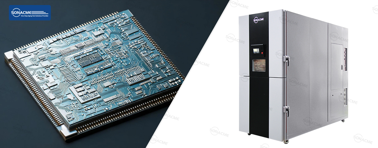
An IC package is a composite structure: silicon die, die attach adhesive, lead frame or substrate, molding compound, and solder balls. Each material has a different coefficient of thermal expansion (CTE). When the package undergoes rapid temperature transitions — say from +125°C to -55°C in seconds — these materials expand and contract at different rates. The resulting mechanical stress concentrates at material interfaces, particularly between the die and the molding compound, and between the die attach and the lead frame.
Over repeated thermal shock cycles, micro-cracks initiate at these interfaces, propagate, and eventually cause visible delamination. The consequences are severe: moisture ingress, electrical discontinuity, and catastrophic field failure.
MIL-STD-883 Method 1011: The Gold Standard for Thermal Shock
MIL-STD-883 Method 1011 is specifically designed to expose delamination risks in microcircuit packages. The test subjects devices to rapid transitions between extreme temperature extremes — typically +100°C to -65°C — with a transition time of less than 10 seconds. The standard requires a minimum of 15 cycles, though many manufacturers run 100+ cycles for qualification.
Key parameters of Method 1011:
- Hot zone temperature: +100°C (Condition A) to +150°C (Condition C)
- Cold zone temperature: -65°C (Condition A) to -80°C (Condition C)
- Transfer time: ≤10 seconds
- Soak time: ≥5 minutes at each extreme
- Post-test inspection: Visual, electrical, and acoustic microimaging
The SONACME Two-Zone Thermal Shock Test Chamber Solution
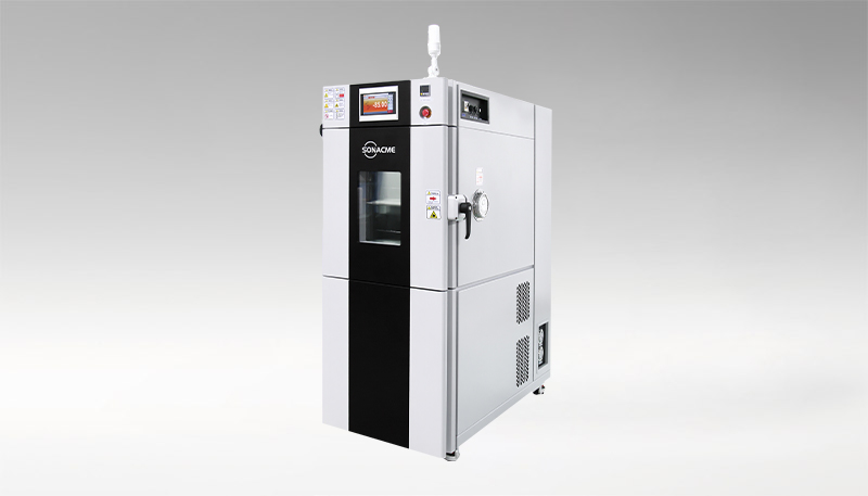
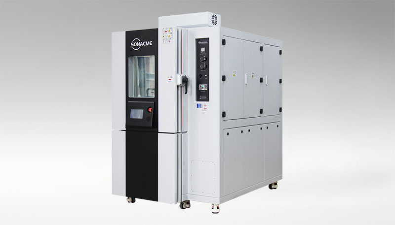
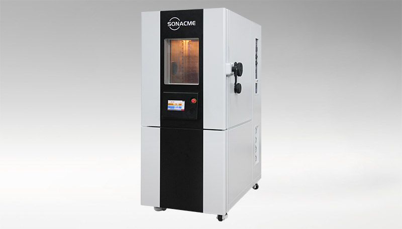
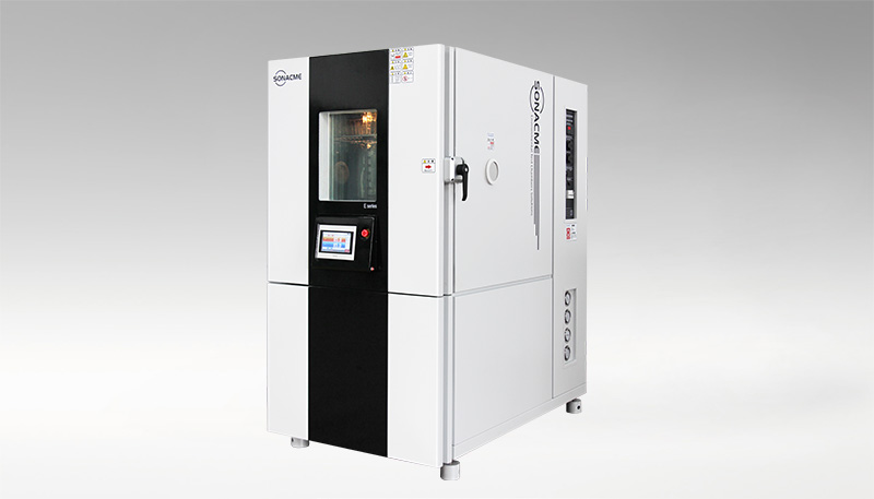
SONACME’s Two-Zone Thermal Shock Test Chamber is engineered to meet and exceed MIL-STD-883 Method 1011 requirements. The chamber uses an elevator-type basket mechanism that physically transfers the specimen between independently controlled hot and cold zones, achieving transition times well within the 10-second specification.
Key Technical Parameters:
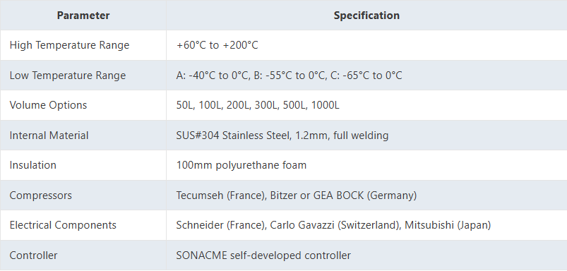
The chamber’s full-welding SUS304 stainless steel inner chamber ensures excellent sealing, preventing condensation cross-contamination between zones. The 100mm polyurethane insulation minimizes thermal loss, stabilizing temperature recovery times.
Practical Application: Semiconductor Package Qualification Workflow
A typical delamination screening workflow using the SONACME chamber involves:
- Pre-test baseline: Electrical test + scanning acoustic microscopy (SAM) to establish reference images
- Thermal shock exposure: 50 cycles per MIL-STD-883 Method 1011, Condition C (+150°C / -65°C)
- Interim inspection: Electrical test every 25 cycles to detect parametric drift
- Post-test analysis: SAM imaging to identify delamination area percentage, cross-sectioning for failure analysis
This workflow typically reveals delamination in packages that pass steady-state temperature cycling but fail under thermal shock — precisely the failure mode that Method 1011 is designed to catch.
Why Thermal Shock Matters More Than Ever
With the shift to advanced packaging technologies — chiplets, 2.5D interposers, and fan-out wafer-level packaging — the number of material interfaces in a single package has multiplied. Each interface is a potential delamination site. Thermal shock testing per MIL-STD-883 Method 1011 is no longer just a military-spec requirement; it has become an essential reliability gate for any advanced semiconductor package.
SONACME’s Two-Zone Thermal Shock Test Chamber provides the precise, repeatable, and certifiable thermal shock environment that semiconductor manufacturers need to catch delamination before it reaches the field. With compliance to MIL-STD-883, MIL-STD-810, IEC 60068-2-14, and JEDEC standards, the chamber is a versatile tool for any semiconductor reliability lab.
Contact SONACME Technology to discuss your thermal shock testing requirements and discover how our chambers can integrate into your semiconductor qualification workflow.
Latest News
-
IEC 60068-2-14 Na/Nb Testin...
MIL-STD-883 Method 1011 thermal shock testing guide ...
-
JEDEC JESD22-A106 Complianc...
MIL-STD-883 Method 1011 thermal shock testing guide ...
-
Meeting ISO 26262 Standards...
MIL-STD-883 Method 1011 thermal shock testing guide ...
-
IEC 60068-2-38 Environmenta...
MIL-STD-883 Method 1011 thermal shock testing guide ...
-
Essential reading for autom...
MIL-STD-883 Method 1011 thermal shock testing guide ...
-
IEC60068-2-30How does a Dou...
MIL-STD-883 Method 1011 thermal shock testing guide ...
+86-180 2704 9206
Tel:+86(0769)83234966
E-Mail:info@sonacme.com
Contacts:Marcia/+86-180 2704 9206
Add:Building 7, No.310 Songbai Road, Liaobu Town, Dongguan City, Guangdong




 +86-180 2704 9206
 WhatsApp:+86-180 2704 9206
 info@sonacme.com