

JESD22-A104 Temperature Cycling: Validating Stacked-Die BGA NAND Flash Reliability
Publish Time:2026-10-14Views:()
Test Standard: JEDEC JESD22-A104 — Temperature Cycling
NAND flash memory has become the backbone of the data storage industry. From smartphones to enterprise SSDs to automotive infotainment systems, NAND flash stores the world's data. And at high density, that memory almost always ships as a BGA — a stack of NAND die wire-bonded to a substrate and sealed in molding compound. JESD22-A104 is the JEDEC standard that defines how to qualify those stacked-die BGA packages under temperature cycling.
The Stacked-Die BGA Challenge: Wire Bond and Solder Joint Fatigue
A modern high-density NAND package — 3D NAND, eMMC, or UFS — is built in BGA (ball grid array) or LGA format: up to 16 NAND die stacked on a BT-resin substrate, each die bonded to the one below with die attach film (DAF), wire-bonded die by die, encapsulated in molding compound, and terminated with a ball grid on the underside. TSOP-48 survives today only for legacy low-density SLC parts; mainstream 3D NAND has moved entirely to BGA and LGA.
This stack-up is a chain of material interfaces, each with a different coefficient of thermal expansion (CTE):
· Die-to-die interface: every die is separated from the next by a DAF layer, so a 16-die stack contains 15 CTE-mismatch interfaces
· Wire bond spans: vertical stacking forces longer wire spans and deeper loop heights, leaving each wire as a free-standing beam inside the package
· Solder ball joints: the ball grid couples the package to the PCB, where copper traces, solder and BT substrate expand at different rates
· Charge retention: not a mechanical failure, but temperature cycling accelerates charge loss in the flash cells and shows up as a rising bit error rate
The primary failure modes under temperature cycling are:
1. Wire bond breakage: occurs mainly at the loop apex, where the arc concentrates stress, and at the bond point to the die, where the ball bond and the pad beneath it take the shear
2. Solder ball fatigue: for BGA packages, the corner balls are most vulnerable — they sit furthest from the neutral point and therefore see the greatest shear strain
3. Molding compound cracking: cracks initiate at die corners and edges, often followed by interfacial delamination between the molding compound and the die surface
4. Die attach (DAF) failure: cohesive or adhesive failure of the film bondline, which opens voids between stacked die
For a stacked-die BGA, the first two mechanisms dominate — wire bonds and solder joints are the weakest links in the thermal fatigue chain.
JESD22-A104: The JEDEC Temperature Cycling Standard
JESD22-A104 defines temperature cycling for solid-state devices. The standard specifies:
Condition | Min Temp | Max Temp | Ramp Rate | Typical Applications |
A | -55°C | +85°C | Natural | Commercial |
B | -55°C | +125°C | Natural | Industrial |
C | -65°C | +150°C | Natural | Military/Automotive |
D | -65°C | +125°C | Natural | Military |
F | -55°C | +125°C | ≤10°C/min | Automotive (powered) |
G | -40°C | +125°C | ≤10°C/min | Automotive AEC-Q100 |
H | -55°C | +150°C | Natural | Extreme screening |
Key requirements:
· Transition time: ≤5 minutes to ramp between temperature extremes
· Soak time: Until the device reaches thermal equilibrium at each extreme
· Cycle count: 500 or 700 cycles (screening) for most applications; 1000+ cycles (qualification); up to 5000 cycles for automotive Grade 0
· Post-test: Full electrical characterization, package X-ray, SAT (scanning acoustic tomography), and cross-section analysis of failed samples
One Method, Two Worlds: Consumer-Grade vs Industrial/Automotive BGA NAND
JESD22-A104 is a test method, not a grade. The same document is called up by consumer, industrial and automotive qualification programs alike — what separates them is how hard the method is run.
Dimension | Consumer-grade | Industrial / automotive BGA NAND |
Method | JESD22-A104 | JESD22-A104 (the same document) |
Condition | A | B, C, G or H |
Cycle count | 100-500 | 1000+ (Grade 1); up to 5000 (Grade 0) |
Parent framework | JESD47 / JEP150 | AEC-Q100 |
Acceptance rule | Statistical fallout permitted | Zero failures, three non-consecutive lots |
The same die in the same BGA package can pass one column and fail the other. Acceptance rules sharpen the gap: a consumer part is allowed a small statistical fallout, while an automotive BGA NAND has to return zero failures across three non-consecutive lots. That is why a consumer-grade part can never be "upgraded" to automotive on paperwork alone — the devices must be re-run at the harsher conditions and higher cycle counts, on a chamber that can hold the profile for weeks without drift.
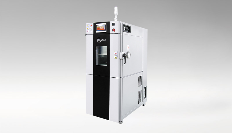
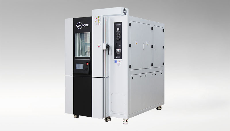
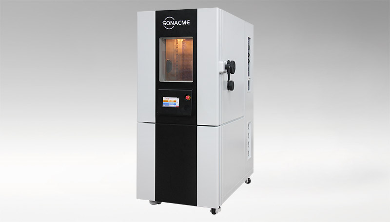
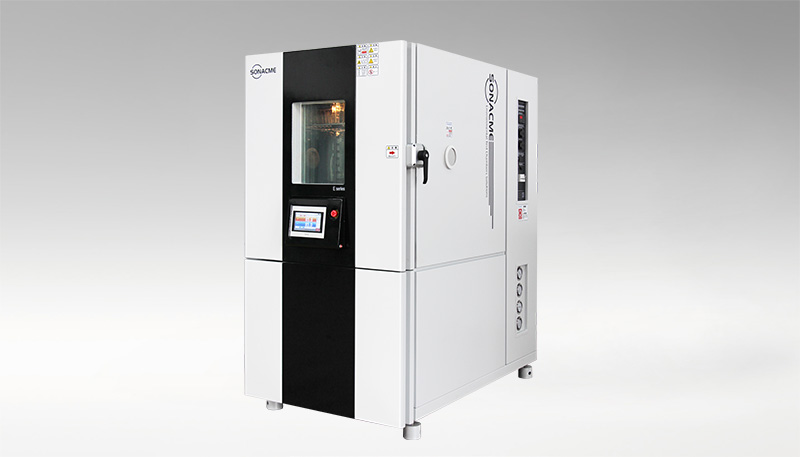
SONACME Rapid Temperature Change Test Chamber for JESD22-A104
SONACME's Rapid Temperature Change Test Chamber is ideal for JESD22-A104 Conditions F and G, which specify a controlled ramp rate — the regime that stresses BGA wire bonds and solder joints most severely. The chamber's programmable change rates of 15K/min, 20K/min, and 25K/min cover the full range of JESD22-A104 requirements, while a uniform air distribution keeps every device in the load within the specified window.
Key Advantages for BGA NAND Flash Testing:
Feature | Benefit for JESD22-A104 |
15-25K/min change rate | Covers Conditions F and G (≤10°C/min) with margin |
Heat load support | Enables powered NAND testing |
Wide humidity range | Supports combined temp/humidity cycling |
Programmable controller | Automated multi-condition test sequences |
LOW GWP technology | 40% energy savings for high-cycle-count testing |
R-449A refrigerant | Future-proof, environmentally compliant |
The chamber's ability to maintain precise temperature change rates is critical for JESD22-A104 compliance. Unlike simple temperature cycling chambers that rely on natural ramp rates, SONACME's chamber actively controls the rate of change, ensuring that every cycle meets the specified ramp rate — a requirement for Conditions F and G.
BGA NAND Flash Temperature Cycling Test Protocol
A recommended JESD22-A104 protocol for stacked-die BGA NAND flash packages:
5. Sample preparation: 45-77 units per lot, pre-test for bad blocks and initial bit error rate (BER), plus an acoustic scan (SAT) to establish a delamination baseline
6. Condition selection: Condition C (-65°C to +150°C) for automotive/military; Condition B (-55°C to +125°C) for commercial/industrial; Condition H (-55°C to +150°C) where a harsher screen is required
7. Ramp rate / Transition time: 5 minutes to transition between temperature extremes
8. Soak time: 15 minutes per extreme (ensures thermal equilibration of multi-die stack)
9. Cycle count: 500 or 700 cycles for screening in most applications; 1000+ cycles for qualification; up to 5000 cycles for automotive Grade 0
10. Interim testing: Read BER and bad block count every 250 cycles
11. Post-test: Full electrical characterization, package X-ray, SAT (scanning acoustic tomography) inspection, and cross-section analysis of failed samples
The SONACME controller supports programming of up to 10 test procedures with 15 segments each, allowing automated execution of complex multi-phase test profiles — including interim room-temperature pauses for electrical testing.
The Future of BGA NAND Reliability Testing
As NAND flash technology advances, 3D NAND layer counts have moved from 176 layers to beyond 300 in mass production, and the newest 400+ layer generations now rely on wafer-to-wafer hybrid bonding. Every bonded wafer interface introduces its own thermal expansion mismatch, and denser QLC storage together with PCIe 5.0 SSDs running at higher power raises the thermal load on the finished BGA package. The industry is also seeing growing demand for automotive-grade NAND in ADAS and autonomous driving platforms, where AEC-Q100 Grade 0 (up to 5000 temperature cycles) is becoming the norm.
JESD22-A104 temperature cycling, executed on a SONACME Rapid Temperature Change Test Chamber, provides the controlled, accelerated environment that BGA NAND manufacturers need to qualify wire bonds, solder joints and die attach for these next-generation applications.
Contact SONACME Technology to discuss your BGA NAND flash temperature cycling requirements.
Latest News
-

IEC 60068-2-14 Nb: Rapid Te...
JESD22-A104 temperature cycling test guide for stack...
-

MIL-STD-810 Method 503 Ther...
JESD22-A104 temperature cycling test guide for stack...
-
IEC 60068-2-14 Na/Nb Testin...
JESD22-A104 temperature cycling test guide for stack...
-
JEDEC JESD22-A106 Complianc...
JESD22-A104 temperature cycling test guide for stack...
-
Meeting ISO 26262 Standards...
JESD22-A104 temperature cycling test guide for stack...
-

IEC 60068-2-38 Environmenta...
JESD22-A104 temperature cycling test guide for stack...
+86-180 2704 9206
Tel:+86(0769)83234966
E-Mail:info@sonacme.com
Contacts:Marcia/+86-180 2704 9206
Add:Building 7, No.310 Songbai Road, Liaobu Town, Dongguan City, Guangdong




 +86-180 2704 9206
 WhatsApp:+86-180 2704 9206
 info@sonacme.com
